Two-inch wafer-scale Micro-QLED fabrication technology
FAYETTEVILLE, GA, UNITED STATES, August 25, 2026 /EINPresswire.com/ -- Micro-QLEDs are emerging as a promising AR

Press Release Disclaimer: This is a press release distributed through the XPR Media network. It has not been independently verified by our newsroom.
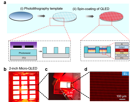

FAYETTEVILLE, GA, UNITED STATES, August 25, 2026 /EINPresswire.com/ — Micro-QLEDs are emerging as a promising AR technology due to their high brightness and high-resolution capability. Scientists in China developed a two-inch wafer-scale fabrication process for Micro-QLEDs which provides a simple and low-cost route to accelerate the industrial application of Micro-QLED display.
Quantum dot light-emitting diodes (QLEDs) have attracted considerable attention for display applications owing to their high brightness, excellent color performance, and solution-processability. As crucial components of AR technology, microdisplay panels have attracted a great number of attentions.
To date, several microdisplay technologies have been developed, including liquid crystal on silicon (LCoS), micro-organic light-emitting diodes (Micro-OLEDs), micro-light-emitting diodes (Micro-LEDs), and micro-quantum dot light-emitting diodes (Micro-QLEDs). However, there are still great challenges to meet the requirements of high resolution and high brightness of AR technology, due to the brightness limitation of LCos and Micro-OLED and the full color limitation of Micro-LED. Micro-QLED are emerging as an alternative microdisplay technology due to their high brightness and solution-processed ability. Therefore, it is important to develop wafer-scale fabrication processing to advance the industrialization of Micro-QLED for AR microdisplay applications.
In a new paper published in Light: Advanced Manufacturing, a team of scientists led by Professor Haizheng Zhong from Beijing Institute of Technology, together with a team of scientists led by Professor Yuren Wang from the Institute of Mechanics, Chinese Academy of Sciences developed a feasible fabrication strategy for 2-inch Micro-QLED wafers by combining solvent engineering and photolithography-template assisted processing. The 2-inch wafer could provide fifteen microdisplay panels of 0.46-inch with a resolution of 2510 ppi (pixel size from 4 to 50 μm). This route significantly advances the practical application of Micro-QLED for AR microdisplay.
“The two-inch wafer-scale Micro-QLED fabrication process consists of two critical steps (Figure 1): (1) fabrication of photolithography templates and (2) spin-coating of QLED.”
“Using this approach, we successfully fabricated a two-inch Micro-QLED wafer with 15 microdisplay panels of 0.46-inch. (Figure 1) The microdisplay panel exhibited uniform electroluminescence, with pixel sizes from 4 to 50 μm and a maximum resolution of 2510 pixels per inch (ppi), demonstrating their potential for high-resolution AR microdisplay applications.” they added.
“During spreading process of quantum-dot droplet, the spreading behavior plays a crucial role in determining film area and uniformity. We found that introducing a hexane/octane mixed solvent could effectively regulate droplet spreading behavior (Figure 2). Because hexane has a lower boiling point and surface tension than octane, the mixed solvent could effectively tune the evaporation behavior and drying dynamics during spin coating. Based on in situ microscopic observations, we illustrated the solvent evaporation-induced surface tension gradient and subsequent Marangoni flow during droplet spreading, promoting outward movement of the three-phase contact line and enlarging the spreading area of quantum-dot ink. The binary solvent system enables uniform QD deposition while suppressing the coffee-ring effect.” the scientists explained. “This strategy provides an effective approach for achieving large-area uniform quantum-dot films for wafer-scale Micro-QLED fabrication.”
“We believe that this approach could accelerate the transition of Micro-QLEDs from laboratory demonstrations toward practical applications. This method will be a significant milestone in the development of microdisplay technologies.” the scientists forecast.
References
DOI
10.37188/lam.2026.091
Original Source URL
https://doi.org/10.37188/lam.2026.091
Funding Information
This work was supported by the National Natural Science Foundation of China (grant number: U23A20683) and Beijing Municipal Science & Technology Commission, Administrative Commission of Zhongguancun Science under Park No. Z231100006023018 and the National Natural Science Foundation of China (grant number: 12272390).
Lucy Wang
BioDesign Research
email us here
Legal Disclaimer:
EIN Presswire provides this news content “as is” without warranty of any kind. We do not accept any responsibility or liability
for the accuracy, content, images, videos, licenses, completeness, legality, or reliability of the information contained in this
article. If you have any complaints or copyright issues related to this article, kindly contact the author above.

Media gallery